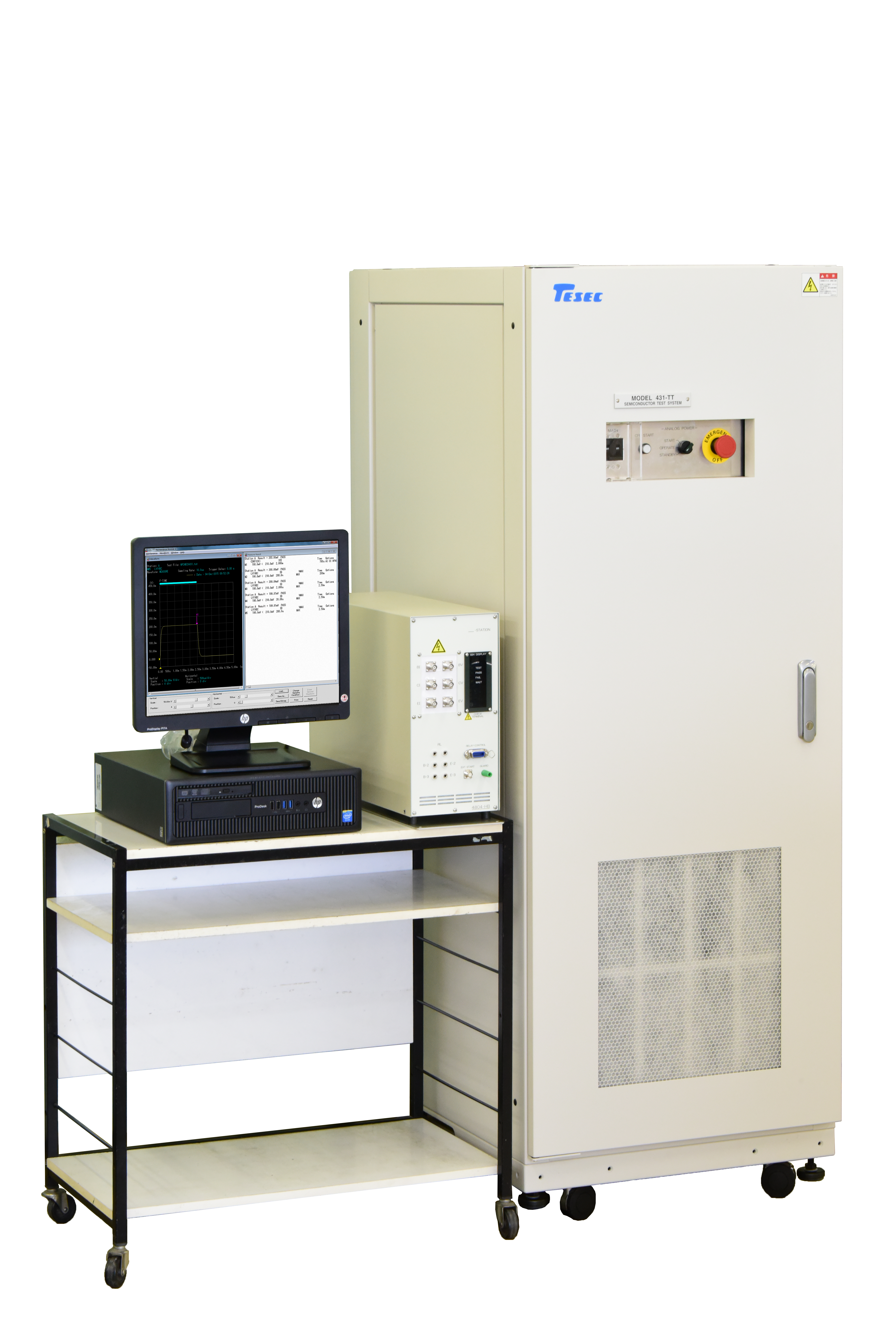




Test Systems

431-TT

431-TT

The 431-TT is a high-performance DC test system supporting static characterization of a wide range of power semiconductor devices, including SiC (silicon carbide), GaN (gallium nitride), IGBTs, MOSFETs, power transistors, and diodes. Covering a broad array of applications from R&D and evaluation to mass production processes, it delivers high-precision, highly efficient characterization of power devices requiring high-voltage and high-current measurement.
The standard configuration supports up to 1.2 kV / 65 A (130 A between C-E), while the expanded configuration supports up to 2.2 kV / 200 A. Adding optional units makes it possible to build a measurement environment capable of up to 10 kV / 1200 A. Meeting the demands for higher breakdown voltages and larger currents in next-generation power semiconductors, it provides an optimal test solution for developing and quality-evaluating devices aimed at EVs (electric vehicles), renewable energy systems, industrial equipment inverters, and power supply units.
In addition, seamless integration with probers and handlers allows for an end-to-end evaluation environment from wafer testing to final testing, achieving both increased productivity and high-quality device evaluation.

Feature

・Support for a Wide Range of Power Semiconductors Including SiC and GaN
 Supports DC characterization of diverse power semiconductor devices such as SiC MOSFETs, GaN devices, IGBTs, FETs, transistors, and diodes. Ideal for R&D and mass-production evaluation of next-generation power devices.

・High-Voltage and High-Current Measurement Capability
 Supports up to 1.2 kV / 65 A in the standard configuration and up to 2.2 kV / 200 A in the expanded configuration, expandable up to 10 kV / 1200 A with external options. Accommodates the evaluation needs of power semiconductors undergoing higher breakdown voltage and higher power output.

・End-to-End Coverage from Wafer Testing to Final Testing
 Combining the system with probers and handlers allows flexible operation from wafer evaluation during development stages to final testing on mass production lines. It supports the integration of evaluation equipment and mass production facilities.

・Increased Productivity via Multi-Device Testing
 Equipped with a multi-device test function supporting simultaneous measurement of 2 DUTs, shortening measurement time and improving inspection efficiency. Contributes to higher throughput in mass production processes.

・Wafer Parallel Measurement Function
 Supports wafer parallel testing via simultaneous measurement of 2 dies, helping reduce evaluation time and lower costs. Delivers a measurement environment suited for mass production inspection processes of power semiconductors.

・High-Speed, High-Precision DC Characterization
 Adopts a VI Source Measure Module configuration to perform static characterization of power devices at high speed and with high accuracy. Efficiently evaluates parameters such as voltage/current characteristics and leakage current characteristics.

 Item

  Specifications

Supported Devices

SiC MOSFET / GaN HEMT, IGBT, Module, etc.

Polarity

NPN / PNP, N / P Channel

Voltage

1.2kV / 2.2kV
(With an additional 10 kV option unit)

Current

65 A C-E: 130 A / 200 A
(With an additional 1200A option unit)

Test Mode / Analog Unit

2  Parallel & 2 Serial (Max)

Number of Analog Unit

2 (Max)

Test Item

999

Sort Item

250

Resolution (Bias)

4 digits

Resolution (Measure)

5 digits