 採用サイト
採用サイト



 日本語
日本語







Products
Product
High-Throughput Wafer Parallel Testing Capability: Supports 8/16 Parallel and UIS Testing
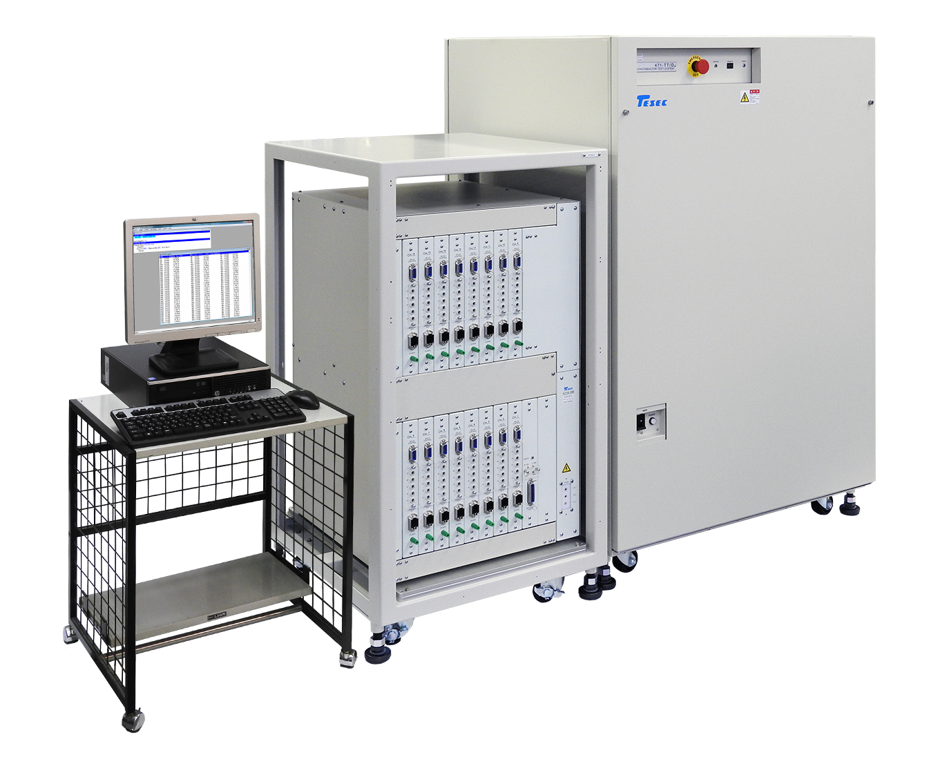
471-TT
471-TT is a DC test system for power devices that enables simultaneous testing of multiple dies in the wafer testing process. Supporting simultaneous testing for 8-parallel and 16-parallel configurations, it achieves a significant throughput improvement compared to conventional single-testing methods. It contributes to enhancing productivity and reducing test costs in the mass production inspection process of power semiconductors, providing a highly efficient wafer testing environment. In addition, inherited from TESEC's accumulated high-voltage and high-current measurement technology, it supports high-voltage application of up to 2kV. It not only enables high-precision evaluation of DC characteristics for various power semiconductor devices such as SiC MOSFETs, GaN HEMTs, IGBTs, and diodes, but also supports avalanche measurement, which is in high market demand. Through this, it assists in quality evaluation, reliability evaluation, and inspection efficiency improvement in mass production processes for SiC devices and next-generation power semiconductors. Furthermore, it supports capacitance measurements such as Rg and Ciss, which are frequently requested. High-speed data transfer via LAN communication and high-speed relay switching functions shorten test times, contributing to tact time improvements across the entire production line. It is the optimal test solution for the high-volume production power semiconductor market, including power semiconductors for EVs, inverters for industrial equipment, and devices for renewable energy applications.
Feature
High-Throughput Inspection via 8-Parallel and 16-Parallel Testing Supports simultaneous testing of multiple dies, significantly improving productivity in the wafer test process. It achieves reduced inspection time and cost reduction in mass production environments.
Integrated UIS and DC Characteristic Testing in a Single Unit In addition to DC parametric testing, it supports UIS (Unclamped Inductive Switching) testing using dedicated units. It can be utilized across a wide range of applications from R&D evaluation to mass production inspection.
Supports High-Voltage Testing up to 2kV Equipped with testing capabilities up to 2kV, essential for evaluating high-voltage power semiconductors. It is also suitable for evaluating SiC devices and high-voltage MOSFETs.
High Test Stability Even in Parallel Testing Through proprietary measurement technology, it achieves stable measurement accuracy even in 8-parallel and 16-parallel environments. It strongly supports quality control in mass production processes.
High-Speed Data Processing via LAN Adoption Adopting a LAN interface shortens data communication times and, combined with faster relay switching, reduces test tact times.
Safety Design Considering Prober and Probe Card Protection Equipped with voltage and current limit control functions to reduce stress on probe pins. Additionally, it automatically divides the number of test dies according to the prober's current capacity, ensuring safe and efficient operation.
Ideal for Wafer Mass Production Inspection Provides a testing environment that balances high productivity and reliability in wafer-level inspection for power semiconductors, IGBTs, MOSFETs, power transistors, and more.
| Item | Specifications |
Supported Devices |
SiC MOSFET / GaN HEMT, IGBT, etc. |
Polarity |
NPN / PNP, N/P Channel |
Voltage |
2kV |
Current |
20 A / 13 A (Avalanche) 200A (Option) |
Parallel Test
|
8 16 (Photo) |
Test Stations |
1 Station |
Test Item |
500 |
Sort Item |
250 |
Resolution (Bias) |
3 digits |
Resolution (Measure) |
4 digits |
-
Contact
-

tel.042-566-1111
8:30 ~ 17:30
 Contact