 採用サイト
採用サイト



 日本語
日本語







Products
Product
DC Static Characteristics and Inductive Load (UIS/Avalanche Ruggedness) One-Pass Test System for SiC/GaN Power Semiconductors
471-TT Version LA
The 471-TT Version LA is a fully automated wafer-level (CP process) test system for power semiconductors, including SiC MOSFETs, GaN FETs, Si MOSFETs, and IGBTs.
In addition to DC static characteristic measurements such as breakdown voltage (Vds/Vdss), leakage current (IDSS), threshold voltage (Vgs(th)), and on-resistance (Rds(on)), the system enables continuous one-pass (single-contact) testing of avalanche ruggedness and avalanche energy under inductive load switching conditions using UIS/UIL (Unclamped Inductive Switching) methodology.
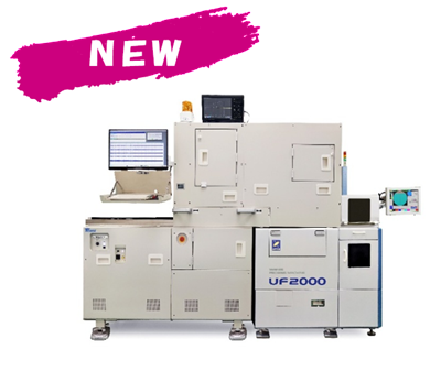
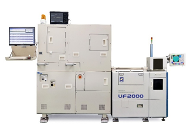
Equipped with high-power test capability of up to 2 kV and 200 A, the system supports volume production inspection and KGD (Known Good Die) screening for both 200 mm (8-inch) and 300 mm (12-inch) wafers. Through full integration with Tokyo Seimitsu wafer probers (UF2000 and AP3000 with DARUMA Chuck), the 471-TT Version LA delivers high-quality and high-efficiency testing solutions for automotive and industrial power devices.
Feature
・Seamless One-Pass Measurement of DC Static Characteristics and Inductive Load (Avalanche Ruggedness)
From high-current, high-voltage DC static characteristic testing to UIS testing (inductive load and avalanche energy ruggedness), the system performs continuous, high-speed automated measurements with a single probe contact. This significantly reduces test cycle time and wafer handling costs.
・High Productivity Through Simultaneous Measurement of Up to Four Chips (Parallel Testing)
Supports multi-site measurements of up to four devices simultaneously at DC 2 kV / 20 A, dramatically increasing wafer test throughput (UPH).
・Ultra-Fast Device Failure Protection (<500 ns)
Even in the event of unexpected device failure during UIS/inductive load testing, such as short-circuit or avalanche breakdown, the measurement circuit is automatically disconnected within 500 ns (nanoseconds). This minimizes physical and electrical damage to probe cards, probe needles, wafers, and test equipment.
・Optimized High-Precision Wafer Test Environment
The combination of the WTS (Wafer Test System), DARUMA Chuck Stage, and Pressurized Card Function suppresses discharge phenomena and contact resistance during high-voltage and high-current testing, ensuring a stable and highly accurate measurement environment.
| Specifications | |
Supported Devices |
SiC-MOSFET, GaN, Si-MOSFET, IGBT, Diode |
Polarity |
NPN/PNP/N-Channel/P-Channel |
| (UIS :Only N-Channel) | |
Test Item |
DC:Vdss, Idss, Vgs(th), Rdson,Vfsd etc. UIS:Avalanche Energy |
Voltage |
2kV |
Current |
200A (DC) /50 ~ 100A (UIS) |
Parallel Test (DC 2kV/20A) |
4 |
Parallel Test (UIS & DC 21A~) |
1 |
Test Stations |
1 |
Test Item |
500 |
Sort Item |
250 |
Resolution (Bias) |
3 digits |
Resolution (Measure) |
4 digits |
Applicable Prober |
ACCRETECH UF2000/AP3000+DARUMA Chuck |
Docking |
Direct Docking |
-
Contact
-

tel.042-566-1111
8:30 ~ 17:30
 Contact